7 Segment LED Displays 102 -- Using a Shift Register © GPL3+
DESCRIPTION
Introduction
This tutorial assumes you are somewhat familiar with 7 Segment LED Displays and builds upon the 7 Segment LED Displays 101 -- How to Make One Work tutorial. To complete this tutorial, you will need the pinout for the 7 Segment LED Display you are using. If you do not have this information, please see the previous tutorial.
Adding one or more shift registers to your project will conserve the number of Arduino compatible I/O pins required to drive your 7 Segment LED Displays and can significantly reduce the power needed for multiple digit displays.
Project Construction
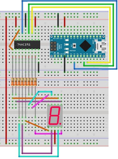
Place one breadboard above the other as shown in the Frizing diagram below. Some breadboards have matching slots and tabs that can be used to lock them together, but this is not essential.
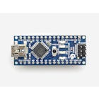
Arduino Uno or Nano Development Board
A 5VDC Arduino Uno or Nano with the ATMega328 microprocessor can safely power this project, driving the 74HC595 Shift Register and Toplite 5161BS 7 Segment LED Display used to develop this tutorial. Any other Single Digit 7 Segment LED Display should be safe to use as long as total current does not exceed 200mA. Leave the development board powered off during project construction.
Connect the 5V pin of the development board to the top power rail of the upper breadboard. Then connect a jumper from that power rail to the bottom power rail of the lower breadboard. Wires connected to the power rails are shown in red. Now connect grounds from the development board to to top and bottom ground rails of the upper breadboard. Wires connected to the ground rails are black.
74HC595 Shift Register
The 74HC595 Shift Register is an integrated circuit (IC) component with a definite notch or dimple at one end. Place the 74HC595 on the upper breadboard with the notch to your left so that the two rows of pins are connected to the breadboard on opposite sides of the center horizontal divide. Any printing on the top of the 74HC595 should appear upright when the IC has been plugged into the breadboard as shown in the above Fritzing diagram.
IC pins are commonly numbered counterclockwise starting with pin 1, which is located to the left or below the dot or notch at one end. The 74HC595 follows this convention. Connect jumpers (shown in red) from the top power rail of the upper breadboard to pins 10 (MR) and 16 (Vcc) of the 74HC595. Pin 16 supplies 5VDC power to the Shift Register and holding Pin 10 (MR) HIGH with 5V prevents the register from clearing.
Connect jumpers (shown in black) from pins 8 (GND) and 13 (OE) to the bottom and top ground rails respectively of the upper breadboard. Pin 8 is the 74HC595 Ground pin and by grounding pin 13, it is held LOW to enable output from the Shift Register.
We will be using pins 4, 7 and 8 on an Arduino compatible Uno or Nano microprocessor development board, although any of the other available I/O pins could be used, if you prefer. The reason I use pins 4, 7 and 8 for shift registers is that these pins don't have any properties other than Digital I/O, so by selecting them, I can reserve the more versatile pins for other uses like interrupts, PWM or various serial and buss communication protocols.
Connect the Arduino compatible development board to the 74HC595 as follows:
- Arduino pin 4 to 74HC595 pin 14 (DS) Serial Data input with a blue wire
- Arduino pin 7 to 74HC595 pin 12 (ST_CP) Latch pin with a green wire
- Arduino pin 8 to 74HC595 pin 11 ( SH_CP) Clock pin with a yellow wire
7 Segment LED Display (single digit)
The particular display used in this tutorial is a TopLite 5161BS with a Common Anode. In order to make this tutorial as general as possible, I will refer to the Display pins by their individual segments (A-G and Dp). Some displays are pinned out the same as the 5161BS, but many are not and others may be of the Common Cathode variety. Do not literally follow the Fritzing project diagram when connecting your display to the 74HC595 shift register. If you are not sure what display pins go to which segments, now would be a good time to review my previous tutorial.
After you have mapped your displays pins to the above segment map, make the following connections:
- 74HC595 pin 15 (Q0) to unused breadboard column next to 74HC595 pin 1 (orange wire)
- From the jumper wire you just installed make a connection to the Display pin corresponding to Segment A using a 330 Ohm resistor. Any resistor value between 180 Ohm to 1,000 Ohm should work as the idea is to protect the Display Segment LED by restricting current.
Using 330 Ohm resistors and jumpers, connect the remaining Display Segments:
- 74HC595 pin 1 (Q1) to resistor then jumper to Display pin for Segment B
- 74HC595 pin 2(Q2) to resistor then jumper to Display pin for Segment C
- 74HC595 pin 3(Q3) to resistor then jumper to Display pin for Segment D
- 74HC595 pin 4(Q4) to resistor then jumper to Display pin for Segment E
- 74HC595 pin 5(Q5) to resistor then jumper to Display pin for Segment F
- 74HC595 pin 6(Q6) to resistor then jumper to Display pin for Segment G
- 74HC595 pin 7(Q7) to resistor then jumper to Display pin for Segment Dp
The last step of the construction phase of this project is to connect a common pin on the Display to either the power or ground rail on the breadboard. If you have a Common Anode Display, use a red jumper to the power rail, otherwise connect a Common Cathode Display to the ground rail using a black jumper. Double check your work and leave the development board powered off.
Programming the Arduino IDE Sketch
The sketch is organized into four main sections; Global Declarations, Setup, and the main Loop followed by two User Defined Functions.
Global Declarations
- Constant Integers are given the descriptive labels dataPin, latchPin and clockPin and assigned the values 4, 7 and 8 respectively. If you are using different pin assignments on your project development board, change the values accordingly.
- A Constant Char (single character) labeled common, is given either the value 'a' for Common Anode Displays or 'c' for Common Cathode. As written, the Sketch is set up for Common Anode Displays. If your Display is of the Common Cathode type, comment out or delete the Common Anode declaration line and uncomment the Common Cathode line. In most cases, this will be the only change necessary for the Sketch to run correctly.
- A Boolean Variable, decPt, is initialized as true. This variable is used to indicate if the Decimal Point Segment (Dp) is to be lit.
Setup
The Setup code block merely initializes the development project board pins associated with the constant values of dataPin, latchPin and clockPin for OUTPUT.
Loop
The Loop code block repeats endlessly until power is shut off or a project component fails or is disconnected.
Every time the Loop begins, the value of the Global variable, decPt, is either true or false. Whatever the value happens to be, it is changed from true to false or vice versa so that the Display's Decimal Point segment is only lit on every other pass through the Loop.
A for loop code block then runs 16 times, incrementing the value of the local integer variable, i, from 0 to 15. Each value of i, is passed to the User Defined Function, myfnNumToBits which returns the local byte value, bits, an eight bit representation of all the Display Segments needed to represent the Hexadecimal value of the variable i.
If decPt is true, the value of bits is modified by setting the Least Significant Bit (LSB) to 1 using the Bitwise OR operator.
The User Defined Function, myfnUpdateDisplay is called with the variable, bits, as an argument. When the Display has been updated by the myfnUpdateDisplay function, the program waits for 1/2 second before incrementing the value of i and repeating the for loop until the value of i is greater than 15; then the whole Loop code block starts over.
User Defined Function
myfnUpdateDisplay is called from the for loop within the Loop code block with a byte argument. Each of the 8 bits in the byte represents one of the Display segments from A to Dp.
For Common Cathode Displays, if a bit value is 1, the associated segment is to be lit, otherwise the bit is 0 and the segment is turned off. The bits need to be reversed for Common Anode displays, so all 8 bit values in the byte are flipped if the Global variable, common equals 'a', changing 1s to 0s and 0s to 1s using the BitWise XOR (^) operator with a B11111111 bit mask.
The Arduino compatible development board latchPin is set LOW before the bits are being sent into the 74HC595's registers. Then the shiftOut(dataPin, clockPin, LSBFIRST, byte) function is called to transfer the bits. Finally, latchPin is set HIGH and the Display should show the appropriate alphanumeric character.
Program control is then returned to the for loop inside the Loop code block.
myfnNumToBits
This User Defined Function acts as a lookup table, accepting a number from 0 to 15 and returns a byte where the bits are a map for the hexadecimal alphanumeric character to be displayed. If an unexpected number is received, three vertical bars will be displayed. A more detailed explanation of myfnNumToBits can be found in the previous tutorial, 7 Segment LED Displays 101 -- How to Make one Work.
The Smoke Test
Check the project wiring one last time before powering up the Arduino compatible development board and uploading the Sketch from the Code section of this tutorial.
 |
| × | 1 | |||
| × | 1 | ||||
 |
| × | 2 | |||
 |
| × | 1 | |||
| × | 1 | ||||
 |
| × | 8 |
Introduction
This tutorial assumes you are somewhat familiar with 7 Segment LED Displays and builds upon the 7 Segment LED Displays 101 -- How to Make One Work tutorial. To complete this tutorial, you will need the pinout for the 7 Segment LED Display you are using. If you do not have this information, please see the previous tutorial.
Adding one or more shift registers to your project will conserve the number of Arduino compatible I/O pins required to drive your 7 Segment LED Displays and can significantly reduce the power needed for multiple digit displays.
Project Construction
Place one breadboard above the other as shown in the Frizing diagram below. Some breadboards have matching slots and tabs that can be used to lock them together, but this is not essential.
Arduino Uno or Nano Development Board
A 5VDC Arduino Uno or Nano with the ATMega328 microprocessor can safely power this project, driving the 74HC595 Shift Register and Toplite 5161BS 7 Segment LED Display used to develop this tutorial. Any other Single Digit 7 Segment LED Display should be safe to use as long as total current does not exceed 200mA. Leave the development board powered off during project construction.
Connect the 5V pin of the development board to the top power rail of the upper breadboard. Then connect a jumper from that power rail to the bottom power rail of the lower breadboard. Wires connected to the power rails are shown in red. Now connect grounds from the development board to to top and bottom ground rails of the upper breadboard. Wires connected to the ground rails are black.
74HC595 Shift Register
The 74HC595 Shift Register is an integrated circuit (IC) component with a definite notch or dimple at one end. Place the 74HC595 on the upper breadboard with the notch to your left so that the two rows of pins are connected to the breadboard on opposite sides of the center horizontal divide. Any printing on the top of the 74HC595 should appear upright when the IC has been plugged into the breadboard as shown in the above Fritzing diagram.
IC pins are commonly numbered counterclockwise starting with pin 1, which is located to the left or below the dot or notch at one end. The 74HC595 follows this convention. Connect jumpers (shown in red) from the top power rail of the upper breadboard to pins 10 (MR) and 16 (Vcc) of the 74HC595. Pin 16 supplies 5VDC power to the Shift Register and holding Pin 10 (MR) HIGH with 5V prevents the register from clearing.
Connect jumpers (shown in black) from pins 8 (GND) and 13 (OE) to the bottom and top ground rails respectively of the upper breadboard. Pin 8 is the 74HC595 Ground pin and by grounding pin 13, it is held LOW to enable output from the Shift Register.
We will be using pins 4, 7 and 8 on an Arduino compatible Uno or Nano microprocessor development board, although any of the other available I/O pins could be used, if you prefer. The reason I use pins 4, 7 and 8 for shift registers is that these pins don't have any properties other than Digital I/O, so by selecting them, I can reserve the more versatile pins for other uses like interrupts, PWM or various serial and buss communication protocols.
Connect the Arduino compatible development board to the 74HC595 as follows:
- Arduino pin 4 to 74HC595 pin 14 (DS) Serial Data input with a blue wire
- Arduino pin 7 to 74HC595 pin 12 (ST_CP) Latch pin with a green wire
- Arduino pin 8 to 74HC595 pin 11 ( SH_CP) Clock pin with a yellow wire
7 Segment LED Display (single digit)
The particular display used in this tutorial is a TopLite 5161BS with a Common Anode. In order to make this tutorial as general as possible, I will refer to the Display pins by their individual segments (A-G and Dp). Some displays are pinned out the same as the 5161BS, but many are not and others may be of the Common Cathode variety. Do not literally follow the Fritzing project diagram when connecting your display to the 74HC595 shift register. If you are not sure what display pins go to which segments, now would be a good time to review my previous tutorial.
After you have mapped your displays pins to the above segment map, make the following connections:
- 74HC595 pin 15 (Q0) to unused breadboard column next to 74HC595 pin 1 (orange wire)
- From the jumper wire you just installed make a connection to the Display pin corresponding to Segment A using a 330 Ohm resistor. Any resistor value between 180 Ohm to 1,000 Ohm should work as the idea is to protect the Display Segment LED by restricting current.
Using 330 Ohm resistors and jumpers, connect the remaining Display Segments:
- 74HC595 pin 1 (Q1) to resistor then jumper to Display pin for Segment B
- 74HC595 pin 2(Q2) to resistor then jumper to Display pin for Segment C
- 74HC595 pin 3(Q3) to resistor then jumper to Display pin for Segment D
- 74HC595 pin 4(Q4) to resistor then jumper to Display pin for Segment E
- 74HC595 pin 5(Q5) to resistor then jumper to Display pin for Segment F
- 74HC595 pin 6(Q6) to resistor then jumper to Display pin for Segment G
- 74HC595 pin 7(Q7) to resistor then jumper to Display pin for Segment Dp
The last step of the construction phase of this project is to connect a common pin on the Display to either the power or ground rail on the breadboard. If you have a Common Anode Display, use a red jumper to the power rail, otherwise connect a Common Cathode Display to the ground rail using a black jumper. Double check your work and leave the development board powered off.
Programming the Arduino IDE Sketch
The sketch is organized into four main sections; Global Declarations, Setup, and the main Loop followed by two User Defined Functions.
Global Declarations
- Constant Integers are given the descriptive labels dataPin, latchPin and clockPin and assigned the values 4, 7 and 8 respectively. If you are using different pin assignments on your project development board, change the values accordingly.
- A Constant Char (single character) labeled common, is given either the value 'a' for Common Anode Displays or 'c' for Common Cathode. As written, the Sketch is set up for Common Anode Displays. If your Display is of the Common Cathode type, comment out or delete the Common Anode declaration line and uncomment the Common Cathode line. In most cases, this will be the only change necessary for the Sketch to run correctly.
- A Boolean Variable, decPt, is initialized as true. This variable is used to indicate if the Decimal Point Segment (Dp) is to be lit.
Setup
The Setup code block merely initializes the development project board pins associated with the constant values of dataPin, latchPin and clockPin for OUTPUT.
Loop
The Loop code block repeats endlessly until power is shut off or a project component fails or is disconnected.
Every time the Loop begins, the value of the Global variable, decPt, is either true or false. Whatever the value happens to be, it is changed from true to false or vice versa so that the Display's Decimal Point segment is only lit on every other pass through the Loop.
A for loop code block then runs 16 times, incrementing the value of the local integer variable, i, from 0 to 15. Each value of i, is passed to the User Defined Function, myfnNumToBits which returns the local byte value, bits, an eight bit representation of all the Display Segments needed to represent the Hexadecimal value of the variable i.
If decPt is true, the value of bits is modified by setting the Least Significant Bit (LSB) to 1 using the Bitwise OR operator.
The User Defined Function, myfnUpdateDisplay is called with the variable, bits, as an argument. When the Display has been updated by the myfnUpdateDisplay function, the program waits for 1/2 second before incrementing the value of i and repeating the for loop until the value of i is greater than 15; then the whole Loop code block starts over.
User Defined Function
myfnUpdateDisplay is called from the for loop within the Loop code block with a byte argument. Each of the 8 bits in the byte represents one of the Display segments from A to Dp.
For Common Cathode Displays, if a bit value is 1, the associated segment is to be lit, otherwise the bit is 0 and the segment is turned off. The bits need to be reversed for Common Anode displays, so all 8 bit values in the byte are flipped if the Global variable, common equals 'a', changing 1s to 0s and 0s to 1s using the BitWise XOR (^) operator with a B11111111 bit mask.
The Arduino compatible development board latchPin is set LOW before the bits are being sent into the 74HC595's registers. Then the shiftOut(dataPin, clockPin, LSBFIRST, byte) function is called to transfer the bits. Finally, latchPin is set HIGH and the Display should show the appropriate alphanumeric character.
Program control is then returned to the for loop inside the Loop code block.
myfnNumToBits
This User Defined Function acts as a lookup table, accepting a number from 0 to 15 and returns a byte where the bits are a map for the hexadecimal alphanumeric character to be displayed. If an unexpected number is received, three vertical bars will be displayed. A more detailed explanation of myfnNumToBits can be found in the previous tutorial, 7 Segment LED Displays 101 -- How to Make one Work.
The Smoke Test
Check the project wiring one last time before powering up the Arduino compatible development board and uploading the Sketch from the Code section of this tutorial.


